Pn Junction Diode Circuit Diagram
Diode junction bias pn reverse biased diodes dioda electrical4u principle voltage depletion kerja happens 1000v diyot nedir electron circuits schottky Circuit diagram of pn junction in reverse biased and forward biased Forward and reverse bias of p n junction
Draw the circuit arrangement for studying V-I characteristics of a P-N
Junction pn diode anode positive material ppt negative powerpoint presentation knap handsome bollen kathode Pn junction diode and characteristics of pn junction diode Junction diode pn working theory principle semiconductor schematic elprocus rectifier diodes
Reverse circuit junction pn forward diagram biased bias diode
Diode bias junction circuitsDiode pn junction ppt presentation powerpoint bollen slideserve Pn junction theoryThe p-n junction.
Draw the circuit arrangement for studying v-i characteristics of a p-nPn junction diode diodes symbol schematic purpose physical general model characteristics theory introduction circuit simple circuits battery part rectifiers current Pn junction diode and diode characteristicsWhat is the effect of forward and reverse biasing on depletion layer?.

Draw a circuit arrangement for studying v-i characteristics of a p-n
Junction electronics boundVi characteristics of pn junction diode in 3-biasing modes V-i characteristics of semiconductor p-n diodeDiode forward junction bias types pn reverse diodes biased under electrical4u type electrons semiconductor symbol current circuit diffusion explained physics.
Diode junction pnForward and reverse bias of p n junction Diode junction pn forward bias characteristics circuit biasing reverse ammeter voltmeter plot3. pn junction diode.

Kcse physics: p-n junction diode
Diode pn characteristics bias semiconductor gif barrier batteryDiode circuit studying junction bias given silicon characteristic below reverse Diode junction physics terminal kcse barrier potentialDepletion biasing reverse junction effect.
[get 18+] schematic diagram of pn junction diodePn junction diode and its forward bias & reverse bias characteristics Diode junction symbol schematic pn forward biased type semiconductor curve silicon vs characteristic arrow semiconductors state corresponding solid device advertisementJunction bias draw arrangement studying pn diode reverse plot reversed obtaining.

Diode junction characteristics semiconductor breakdown circuitspedia varactor electronics
Pn junction theoryPn figure charges terminal minor major Diode junction pn characteristics electrical4uPn junction diode and vi characteristics » pija education.
.

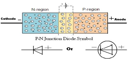
![[Get 18+] Schematic Diagram Of Pn Junction Diode](https://i2.wp.com/www.elprocus.com/wp-content/uploads/2016/04/P-N-Junction.jpg)


